Hello i Have ,defined 50uA idial current source which is suppose to flow straight to diode connected mosfet bellow.The other side of the current source connected to VDD.
As you cant see bellow , all the transistors expect one are saturated,so the transistor is not in cuttoff.The whole 50uA supposed too run threw both series connected transistors .
We are generating custom eye mask for different voltages and data rates. we want to make the eye diagram co ordinates generic. so we used variables in the coordinates. I am using the 6.1.7 version.
These points are middle ones in hexagon shape eye mask. After using the variables we are seeing rectangular waveforms. Can you please help me out how to use the variables in eye mask's co ordinates.
Hello , I am trying to make a Vout/Iin frequency response for the current mirror shown bellow.In the DC region the current mirror workes great.
In order to make AC reponce for Iin/Vout i have added 1 to the AC source,on the output i have not changed the DC source and it stayed 0.5 V DC just to set the bias point for the output transistor.
After that i have defined an expression using calculator IF(In_node)/Vf(out_node) as shown bellow.
However i get a zero plot threwout frequency range.
Where did i got wrong defining the sources or expression in order to get the frequency response of Vout/Iin?
Hello, I'm doing a transistor level PLL simulation for the first time and i'm getting this error:
Image may be NSFW. Clik here to view.
and this is the PLL circuit:
Image may be NSFW. Clik here to view.
from similar posts and answers here I got that one reason might be is saving a lot of signals, but I didn't save more than 5-6. and I didn't also save currents.
the simulation is 4[us] long.
While wondering what might be the reason for that error, could mixing RF transistors (egnfet_rf) and non-RF transistors (nfet) in different blocks in the system might cause a problem?
one thing left is checking with my University adviser if we're not talking about Disk Storage issues. but I don't think this is the case because I emptied a lot of space.
since the last post I've seen about the subject was 2 years ago, does the solution for this problem is more clear now? I'd be glad for suggestions how to solve the problem.
Hello , I am trying to validate my output impedance plot with the OP parameters of the mosfets connected to the output.
the Cds and Cgd capacitances were shown in the zoomed plot bellow.
i have made an Idc source with AC=1V only. and plotted the imaginary part of the output node shown bellow wher Z_ac=V_ac/I_ac
imag(vfreq('ac "/net18")) shown bellow.
However if we look at the imaginary part of the impedance and we see capacitance profile from the output Z_c=1/jwc then the plot should descend,instead it stays constant and starts to rise as if it was and inductor after 10M.
I tried to extract the capacitance from two points i notated on the plot bellow and both of them doesnt match the 10fF capacitance we should have.
Where did i go wrong matching the capacitance from the plot with the capacitane from the OP?
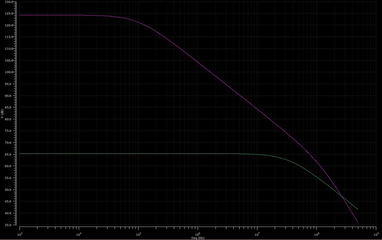
Hello, I have built a closed loop amplifier and tested the gain and phase from the output to the minus input AC=1v source.I got about 70 degrees phase at 0dB amplitude,as shown in the plot bellow.
Afterward i placed an idial current source in the feedback loop, and set STB simulation as shown bellow ,pointing the current source as probe instance.
When i ran the simulation it gives me an error shown bellow that phase marging could not been calculated.
Where did i go wrong setting STB simulation? Thanks.
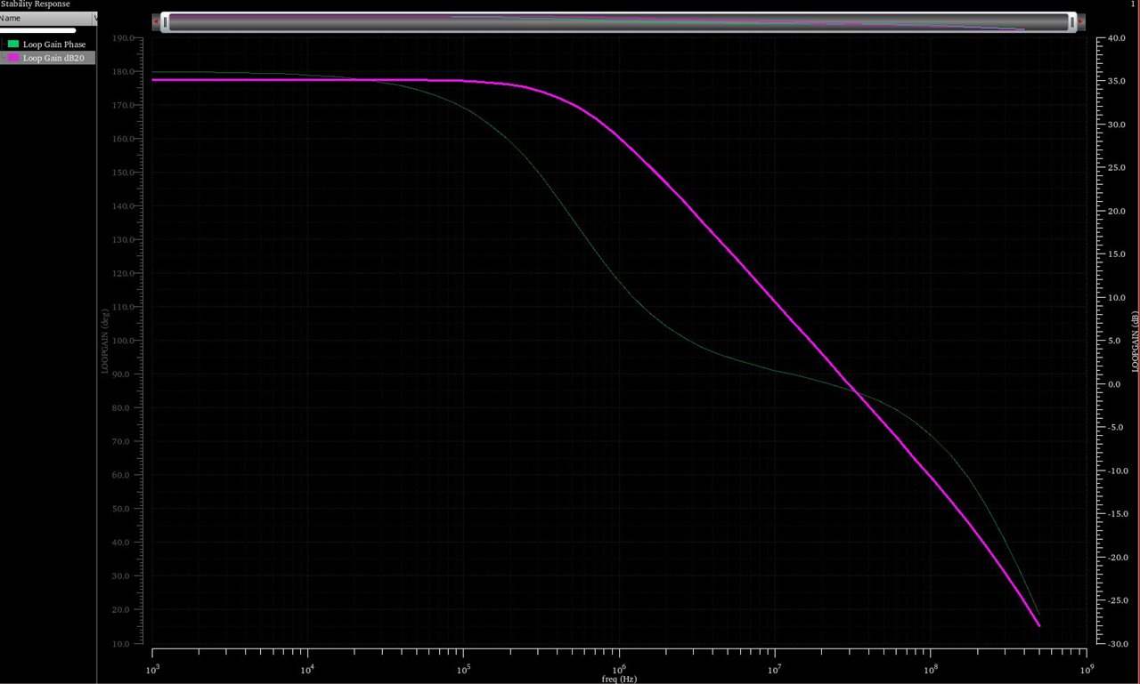
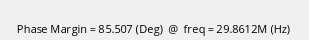
Hello, I ran succsefully STB analysis of a single ended amplifier by connecting Iprobe on the feedback loop shown bellow.
Afterwards i have built a differential amplifier which has common mode feedback(differential feedback), a current probe was connected like before on one of the feedback connections as shown bellow marked with red arrow.
However it gave me an error shown in the end.
Where did i go wrong connecting the probe on differential feedback,for the STB analysis?
Thanks
Single ended feedback:
Image may be NSFW. Clik here to view.
Image may be NSFW. Clik here to view.
Image may be NSFW. Clik here to view.
Differentail beedback:
Image may be NSFW. Clik here to view. Image may be NSFW. Clik here to view.
Hello, I am trying to create an expression which is a combination of regular currect with OP gm. f(gm/id,vgs)
All the manuals which i found are envolving a file system manipulation for creating such expression,probably because they worked with old version.
I made Id vs gs DC sweep and I have tried to create such expression using calculators OP button and dividing it which the Id current expression shown bellow.
It gives me eval error although its a straight forward dividing.
Where did i go wrong?
Thanks.
Image may be NSFW. Clik here to view.
Image may be NSFW. Clik here to view. Image may be NSFW. Clik here to view.
Hello, I have built and amplifier which acts exactly like in the open loop behavior where the gain reduces as the bandwidth increases by the LOOP GAIN factor.(As shown bellow)
However when i calculated the LOOP GAIN i should have OPENLOOP=CLOSED_LOOP+Loop_gain.
Then i remmembered what Andrew said that by removing the loop we change the conditions .
Is there a way in STB to plot OPEN LOOP GAIN and Closed Loop Gain?
So in the same situation i will get OPENLOOP=CLOSED_LOOP+Loop_gain.
An error in the flicker noise model of some devices has been found that leads to incorrect results in pnoise, hbnoise and transient noise analysis. Details can be found at https://designers-guide.org/forum/YaBB.pl?num=1579133686. Cadence R&D are already looking into this.
I am currently trying to power an LNA with a rectifier (AC-DC). the rectifier takes 10us to charge and settle. The problem is when running transient, after 10us the LNA does show gain (20db), but in S21 it has little to no gain (1db).
This is because the sp and dc analysis are running at 0 seconds before any charge is in the rectifier. I am not sure how to make S21 run after 10u. I am also thinking since there is no Vdd (DC supply voltage) the DC analysis is not running properly.
The reason for running SP is to plot my NF and S21.
Am I missing something or not using the correct simulation?
I am simulating a 32.768 kHz Pierce oscillator for phase noise. I have attached the details of my PSS+PNOISE setups in screenshots. Post completion of the analysis, I am unable to get the Direct PLot Main Form to plit the phase noise and get the message in the subject.
One more query query that I would like to be addressed is which of the two analysis, PSS or HB is suited to my design. Now I know that HB gives good results for linear and weakly non-linear oscillators (LC, Colpitts, pierce, etc) and PSS (shooting) for strongly non-linear like ring. The thing is although my osc is a Pierce Oscillator which generates sinusoidal or nearly sinusoidal outputs , I am driving a comparator with these sinusoidal outputs to get a square wave output. Does this imply that I need to use PSS (shooting) if want to see the phase noise/jitter at comparator output and HB if looking for phase noise at osc outputs (with sinusoidal waveforms).
By the way, what is the penalty to be paid if PSS shooting is used for linear and weakly non-linear oscillators?