I need to have over 400 instances of vsource as a pwl in my design with the input to the pwl specified as a csv file. I want to pass the csv file as variable for each instance with variable names like var1, var2, var3 and so on. My question is, is there a way to create multiple instance of vsource at once wherein the file name for instance is automatically incremented as var1, var2 as I keep placing the instances? Going over each instance & typing out the variable name is a lot time consuming.
1) I am trying to measure the IP3 of a mixer that mixes a sin wave with a pulse wave. So can i use PSS + PAC to measure IP3 of this circuit or I have to use QPSS+QPAC.
2) If I have to use QPSS + QPAC, how can I fix the error QPSS did not convergence
Hello, I have designed an impedance matching circuit to adapt an antenna.
I would like to test the entire schematic by inputting different powers through the input port, such as -10dBm or -20dBm, and seeing the S11, S12, etc. through a graph. How can I do this?
Hopefully, this is the correct forum to ask this question. If not, I apologize and ask to be directed to the proper forum.
I am now using AWR microwave office under the evaluation license. I would like to know about the benefits of PDK reuse as described in the linked video.
Perhaps my question is too simplistic but stated this way:
if Microwave Office can import a PDK from some semi conducer manufacturer (just as Virtuoso would), which would have all of the cells that would be available in that process, then I can do the actual RFIC layout in Microwave Office, as well as all of the simulation required. If that is so, why then, would I want to export that design, along with the non static PDK back to Virtuoso?
My only answer to this question would be to be able insert cells, devices, etc. into the design which would not be available in the original PDK but which would have to be developed in Virtuoso.
I'm trying to do a Non-Linear Stability Analysis in AWR MWO 17. While plotting Input/Output Gamma using Gamma Probe (Closed Form): GPROBE2, getting an error saying .AP_HB:NLGAM_GP2(GPROBE2.GP1,1,50,0) : This measurement requires a license to run.
Hello, I am working in a project for fault injection and simulation. Currently, I am using ADE assembler 20.1 version. I want to inject custom open fault in the circuit. I want to know if this is possible with the version 20.1 or not? If yes, any help in this regard would be highly appreciated.
And the second test "dc2" uses a calcVal function dependent on "dc1":
Image may be NSFW. Clik here to view.
"vdc_at_3mA" is an output expression calculated using "sweeps" EvalType in test "dc1":
Image may be NSFW. Clik here to view.
Then I run these two tests for multiple corners, for example, typical, slow & fast.
For each corner, "vdc_at_3mA" output is calculated in test "dc1" & then fed to "dc2" as expected. No issues so far.
However, for whatever reason, if one of the corners take long to converge in test "dc1", "dc2" test does not initiate also for the corners which have converged & finished, until "dc1" is completed for all corners.
For example, say "dc1" test finishes in:
a) 2 minutes for typical corner,
b) 3 minutes for slow corner,
c) 75 minutes for fast corner,
the "dc2" simulation will start only after 75mins also for typical corner, although all the required data for "dc2" test to start in typical corner is available after 2 minutes.
Could you please advice me on this problem? Is there a way to let "dc2" start as soon as "dc1" simulation of a given corner is finished, rather than waiting for all corners to finish.
Please note that I've given a simplified example here. In the actual scenario, I use a transient simulations and therefore using an internal sweep parameter within the test itself is not an option (which could be a potential solution for dc simulations).
my system has a ISV certified GPU. Other design software are able to use the CUDA processing feature. But I'm unable to find any such option in the AWRDE.
I have a frequency multiplier driven circuit (x2) and would like to plot the phase noise for one edge only (as if I used sampled jitter). I have read the thread in
in which it is concluded that the correct way for PSS + pnoise simulation is to use sweep=relative (rel-hr=2 in my case). This is available in noisetype=timeaverage, therefore cannot plot separately raising or falling edge phase noise.
I assume noisetype=sampled (jitter) is not the correct tool here, as it will ignore one rising and one falling edge of the output waveform in the PSS period.
So what is the correct way of getting separate raising/falling edges contributions?
I have been having what seems to be an abnormal amount of trouble using vectors obtained from data files in AWR Microwave Office (v16.03r). I'm attempting to plot the impedance of a transformer I measured using measurements taken from output equations, but I'm getting the error "Equation Error: Data file not found" as pictured here:
Image may be NSFW. Clik here to view. I've dug through the User Guide and formatted the text in the data file (namely column headers) to match the suggestions there. Here it is: community.cadence.com/.../WEX.txt That's data for a Wurth Electronik 750315839 measured using an old HP 4291A impedance analyzer for those interested.
I'm fairly certain that microwave office recognizes that I'm pointing to this file, which is clearly there under "Data Files" in my project view, given that I can rename it with "Synchronize" checked and the data file name will change accordingly in the very output equations I'm trying to use it in. I've gotten this kind of thing to work before using Ls and Q measurements from the same analyzer as parameters in the INDQP model after some similar formatting and identical usage of datafilecol, but it's painful every single time and I've been unable to get it to work in this instance.
I'd love to have a bit more insight into why the error I'm seeing is appearing, since I kind of doubt that MWO is actually unable to find the data file. It could be something as simple as trying to graph the data in the wrong way - I have no idea.
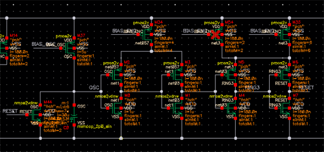
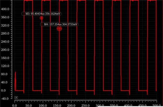
There is an oscillator part in my circuit. The pulse signal generated by the first ring oscillation part has a width of about 31us.Image may be NSFW. Clik here to view.Image may be NSFW. Clik here to view.
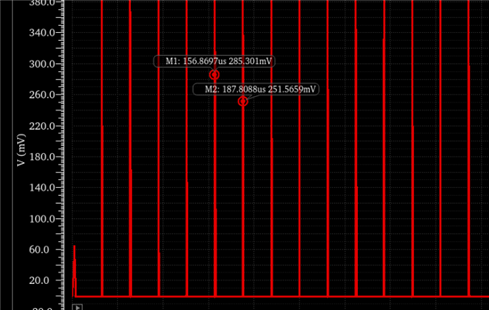
Using this oscillator, some oscillation signals are subsequently generated with a period of about 62us,Image may be NSFW. Clik here to view.
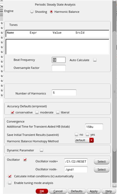
which is used back into the amplifier part. I want to know how to set it during pss simulation, and whether the input port needs to set a frequency. Should I choose shooting or hb, which one should I choose as the oscillation pin, and how to determine the beat frequency. I have set it up many times but it still shows variance errors. I am a newbie looking for help. Thank you very much.Image may be NSFW. Clik here to view.
I am a student learning to use Cadence' s suite of tools. I wonder how to evaluate the large-signal stability of power amplifier using Cadence' s design tools.
I know that Keysight's ADS software offers a method called WSprobe for assessing the large-signal stability of power amplifiers. But I am also interested in whether Cadence's suite of tools provides a similar functionality or if there are alternative, more effective methods for large-signal stability assessment. I have found that the Kf method is not suitable for our complex circuit, so I am seeking alternative solutions to ensure the stability of our circuits.
If such tools are available in Cadence, I also want to know the detailed information on how to use them, as well as their advantages and limitation. If there are no similar tools within Cadence's offerings, I would also like to know if there are any alternative suggestions or techniques that can help us effectively assess the large-signal stability of power amplifiers using Cadence tools.
Used to use Microwave Office extensively ten years ago, but have been in the field so my modeling skills are little rusty.
I am capturing linear S parameters from a Vector Network Analyzer which is driving a SP6T switch
As I cycle through the various switch ports, I want to display the S11 mag (dB) and Phase (DEG) of subsequent iterations.
My real goal is to use a type of Trace Math, wherein in my initial S11 data is the Golden state, and every next trace is compared to the normalized Golden Trace
I've been working with the support team, but something is getting lost in back and forth.
Hi, My virtuoso and spectre version: ICADVM20.1-64b.NYISR30.2 When I want to check a voltage inside the hierarchy, I usually use a deepprobe. For example, in a schematic view, I type "I0.ICH_I.I_OPAMP_RC.I11.vip" in a Hierarchical Node of the instance deepprobe from analogLib and it brings me the node vip to the top level. Now if I want to do the same in an extracted view, if I use a DSPF file, I type: "I0.XICH_I\/XI_OPAMP_RC\/XI11\/vip" and it again shows me the net voltage. I added an "X" in front of the cell name and used "\/" instead of ".". I got this syntax from my colleagues and it works. If I want to see the DC operating point of a device, say region or Vth, I use the following expression in the Assembler: OP("/I0/ICH_I/I_OPAMP_RC/I11/Mip" "region"). Now here comes my problem: I don't know how to modify the expression so I can do the same in the PEX (extracted view). I modified the expression by adding X etc. and tried different variations and it didn't work. I tried to locate the device in the DSPF file and saw the name MMip (instead of Mip). I tried that and it didn't work. If you are familiar, can you please help me with how can I do it? I'm particularly interested to see the device "Vth" after extraction and check if it changes compared to the schematic. I'm not sure how can I properly (syntax) refer to the device in the hierarchy. Thank you.
I'm trying to make a parametric simulation of a PCELL using EMX. Something similar to what is reported here.
Image may be NSFW. Clik here to view.
Basically, I'd like to make a parametric simulation in EMX of a PCELL like the inductor shown in the figure. Is there any way to do it and to show results in an aggregated plot?
Hello everybody, now I am using harmonic balance analysis to determine the optimum load impedance of Power Amplifier, In harmonic balance analysis panel, right click the compression
Image may be NSFW. Clik here to view.
Then after the netlist and run, in the direct plot->main form, can see the xdb options, choosing it and can plot the compression point contour, the result shown below
Image may be NSFW. Clik here to view.
From this plot it's can be seen that when the load impedance Zd=7.44+j4.78, the output compression 1dB Power is 28.2618dBm
But when I directly set the load port impedance equal to 7.44+j4.78, and then sweep pin from -20 to 30dBm, to see the output compression 1dB Power, the result is hugely different, as the graph shown below, this time the simulated result is 30.416dBm
Image may be NSFW. Clik here to view.
I don't know why, can anybody gives me a help, thank you very much!!